
Page 20 - Microelectronics and Semiconductor Materials at TU Dresden
P. 20
NaMlab gGmbh and Chair of Nanoelectronics
Semiconductor technology forms the basis for all The required means for fundamental research in this
electronic devices we rely on in our daily lives. Dresden area is significantly lower than in industry. However, it
became the center of the European semiconductor is still rather expensive, as cleanroom infrastructure is
industry after 1990. This technology therefore show- usually necessary for complete process chains involving
cases Dresden’s unique selling point, which must be a large number of individual devices. The cleanroom
buttressed by fundamental research. laboratory at TU Dresden is operated by the Chair of
Nanoelectronics at the Institute of Semiconductors
and Microsystems, which covers training, including the
cleanroom practical course, as well as research on in-
dividual process topics such as atomic layer deposition,
and perhaps in the more distant future, devices based
on 2D materials.
An important development was the addition of NaMLab
(a 100% subsidiary of TU Dresden) in 2006, which estab-
lished an efficient organizational system to finance the
costly research process using institutional funding (about
15% of the budget) and a full cost model. NaMLab has
catapulted Dresden to a top position in the international
league of semiconductor research in the last five years.
CONTACT This has been achieved in particular through the con-
ception of ferroelectric devices based on hafnium oxide,
Prof. Thomas Mikolajick which is currently considered to be one of the most
Chair of Nanoelectronics // important innovations in the field of materials research
TU Dresden for electronics.
✉ thomas.mikolajick@tu-dresden.de
tu-dresde n.de/ing/elektrotechnik/ihm
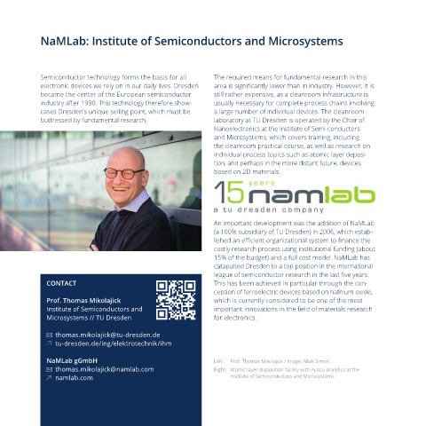
NaMLab gGmbH Left: Prof. Thomas Mikolajick / Image: Maik Simon
✉ thomas.mikolajick@namlab.com Right: Atomic layer disposition facility with in-situ analytics at the
namlab.com Institute of Semiconductors and Microsystems